Samsung Electronics, the world's largest memory chip manufacturer, has introduced a new memory architecture named zHBM, designed for next-generation AI servers. The announcement was made at the Future of Memory and Storage (FMS) 2026 expo in Santa Clara, California. According to preliminary specifications, zHBM offers data transfer speeds up to eight times faster than HBM5 standards, which have not yet entered mass production. This solution aims to overcome data transmission bottlenecks in AI systems, where memory access speed is often the limiting factor.
Three-dimensional design revolutionizes chip-to-chip communication
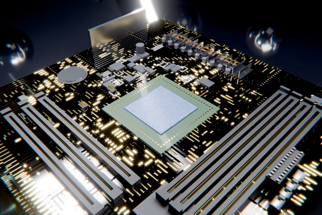
The core innovation of zHBM lies in its Z-axis structure. Unlike traditional HBM configurations, where memory modules are placed horizontally next to the processor on an interposer, zHBM stacks memory chips directly on top of the AI accelerator. This vertical arrangement drastically reduces the physical distance between memory and processor, speeding up data exchange and reducing latency. Samsung claims that memory density is ten times higher compared to HBM5, thanks to advanced wafer bonding technologies that allow more cell layers to be integrated in a smaller footprint.
Sponsored Protocol
Superior energy efficiency and thermal management
In addition to speed, zHBM promises significant improvements in energy efficiency, with power consumption reduced by approximately two-thirds compared to current solutions. Thermal resistance is also 50% lower, a critical aspect for data centers handling intensive AI workloads. This dual advantage could translate into lower operational costs and greater sustainability for high-performance computing infrastructures.
Customization for enterprise clients and launch timeline
Another distinctive feature of zHBM is the ability to integrate custom components in the intermediate layer between accelerator and memory. This flexibility allows clients to optimize the system for specific workloads, further increasing memory capacity and accelerator performance. Samsung has not announced a launch date, but it is likely that zHBM will hit the market after the introduction of HBM5, expected in 2028. Consequently, large-scale commercialization may occur beyond that date.
Sponsored Protocol
This innovation comes during a period of strong growth for the AI memory sector. Companies like NVIDIA and AMD are pushing for ever faster and more capable solutions. Samsung, with its leadership in the memory market, aims to consolidate its position, also in light of the growing demand for AI chips. To better understand the impact of these technologies, it is useful to consider developments in hybrid connectivity systems like Starlink Mobile, which together with new memory solutions could enable distributed AI infrastructures. The challenge, however, is not only technical but also ethical, as highlighted by recent discussions on AI agent behaviors.
Sponsored Protocol
For industry watchers, the arrival of zHBM represents a remarkable step forward. According to experts, memory density will be crucial to support large language models and real-time inference applications. Samsung has already proven its ability to innovate in this field, and with zHBM it raises the bar even higher. For technical details, one can consult the official documentation from Samsung Semiconductor.
Source: https://www.sammobile.com/news/samsung-zhbm-memory-chip-concept-8x-speed-versus-hbm5